Contents
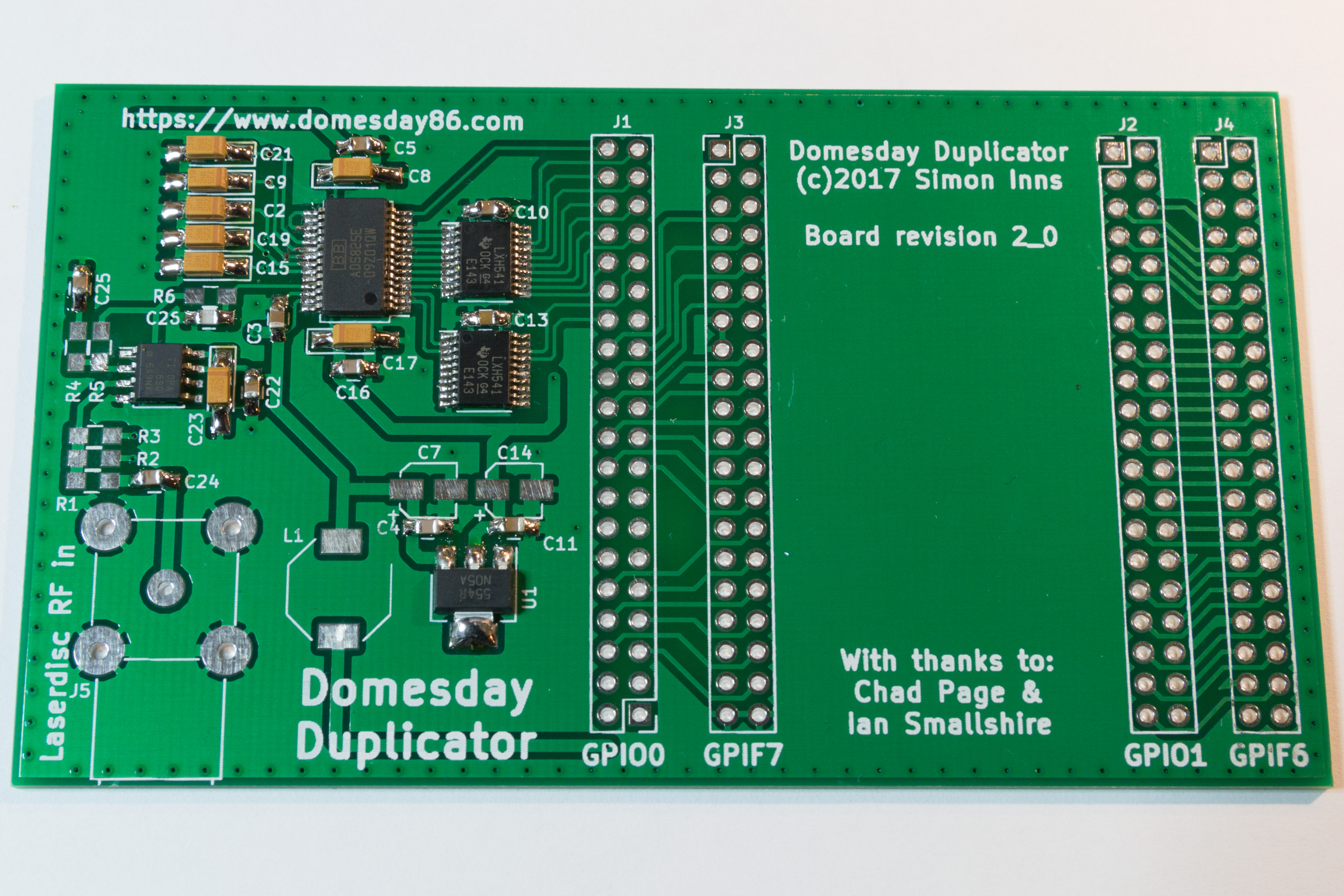
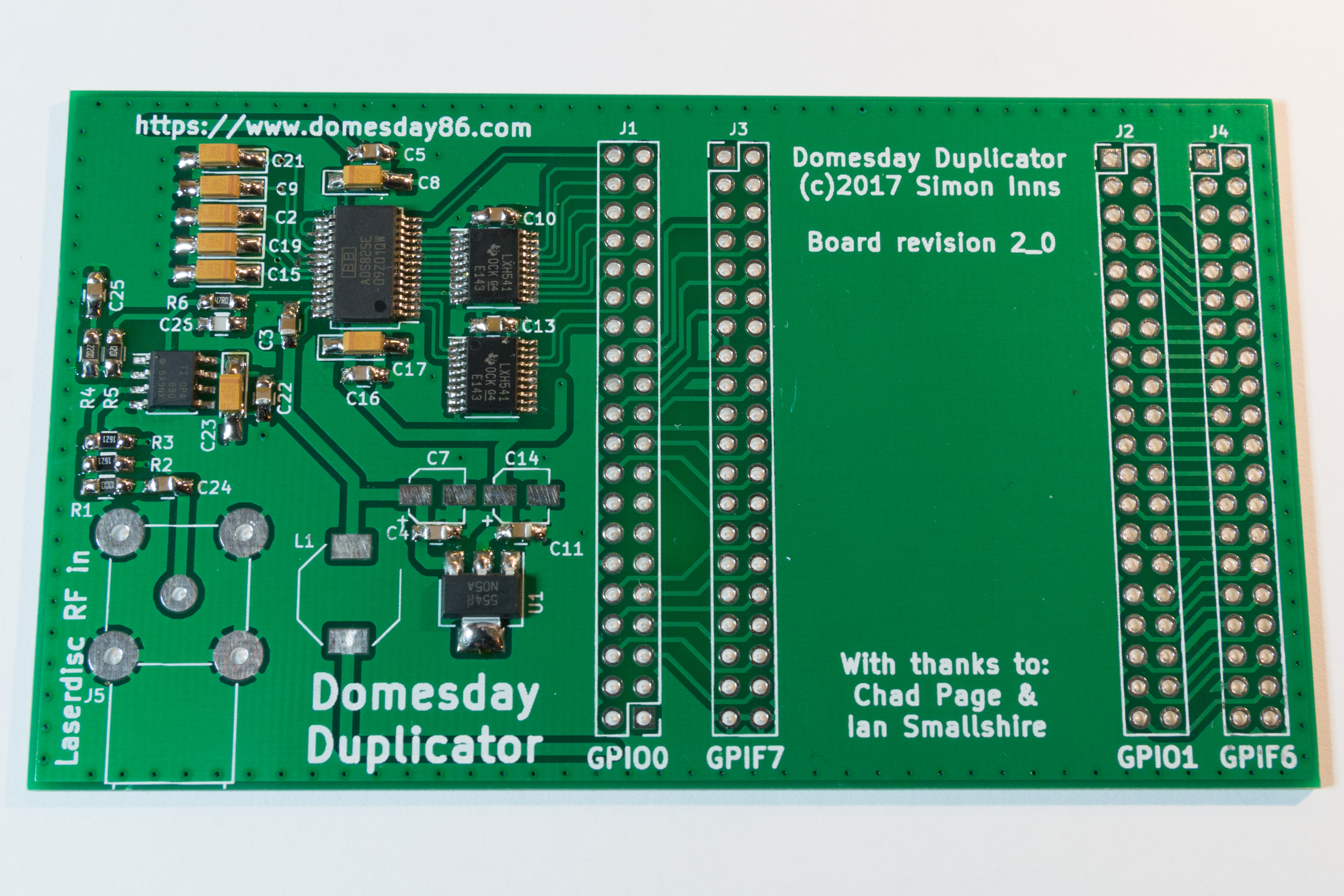
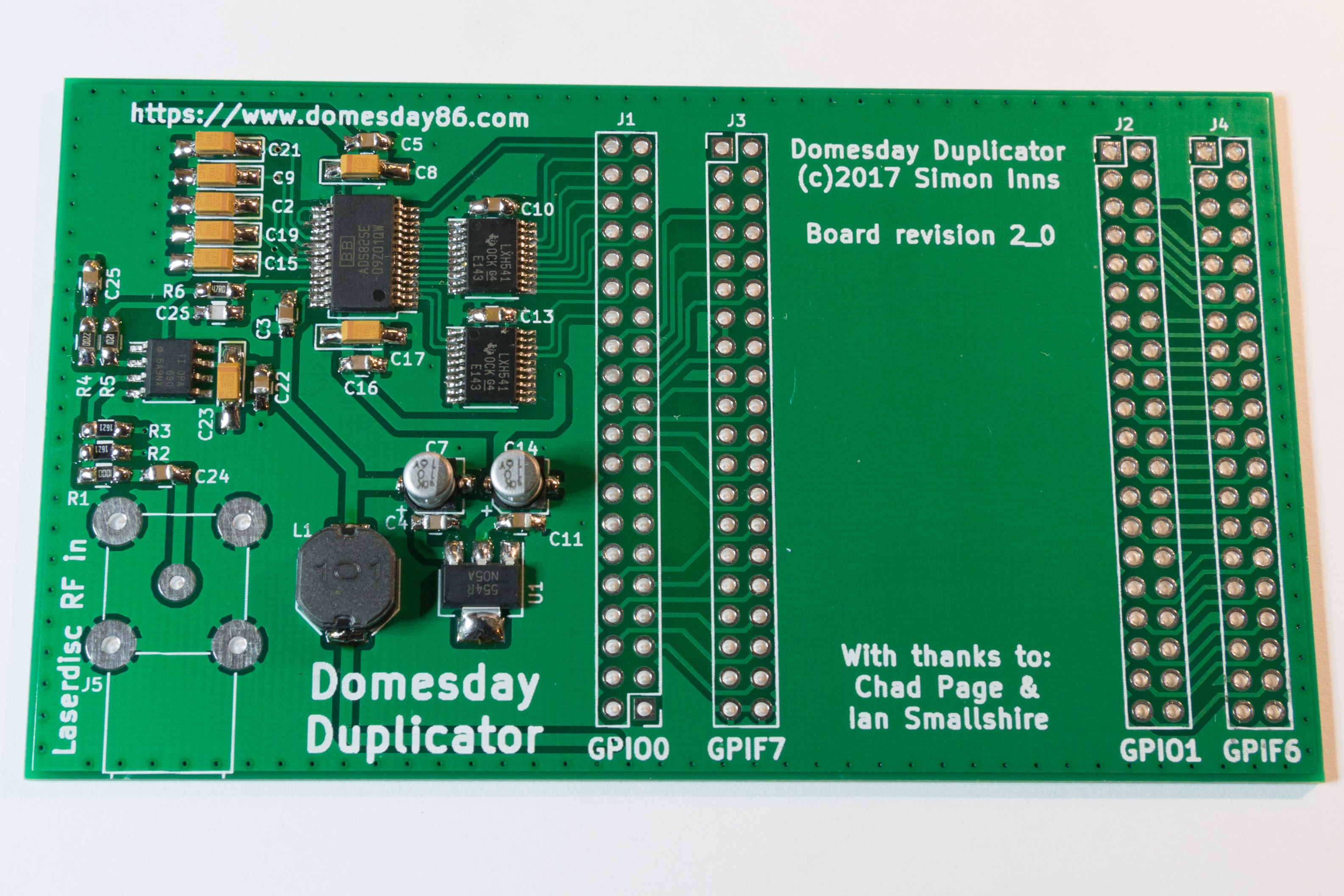
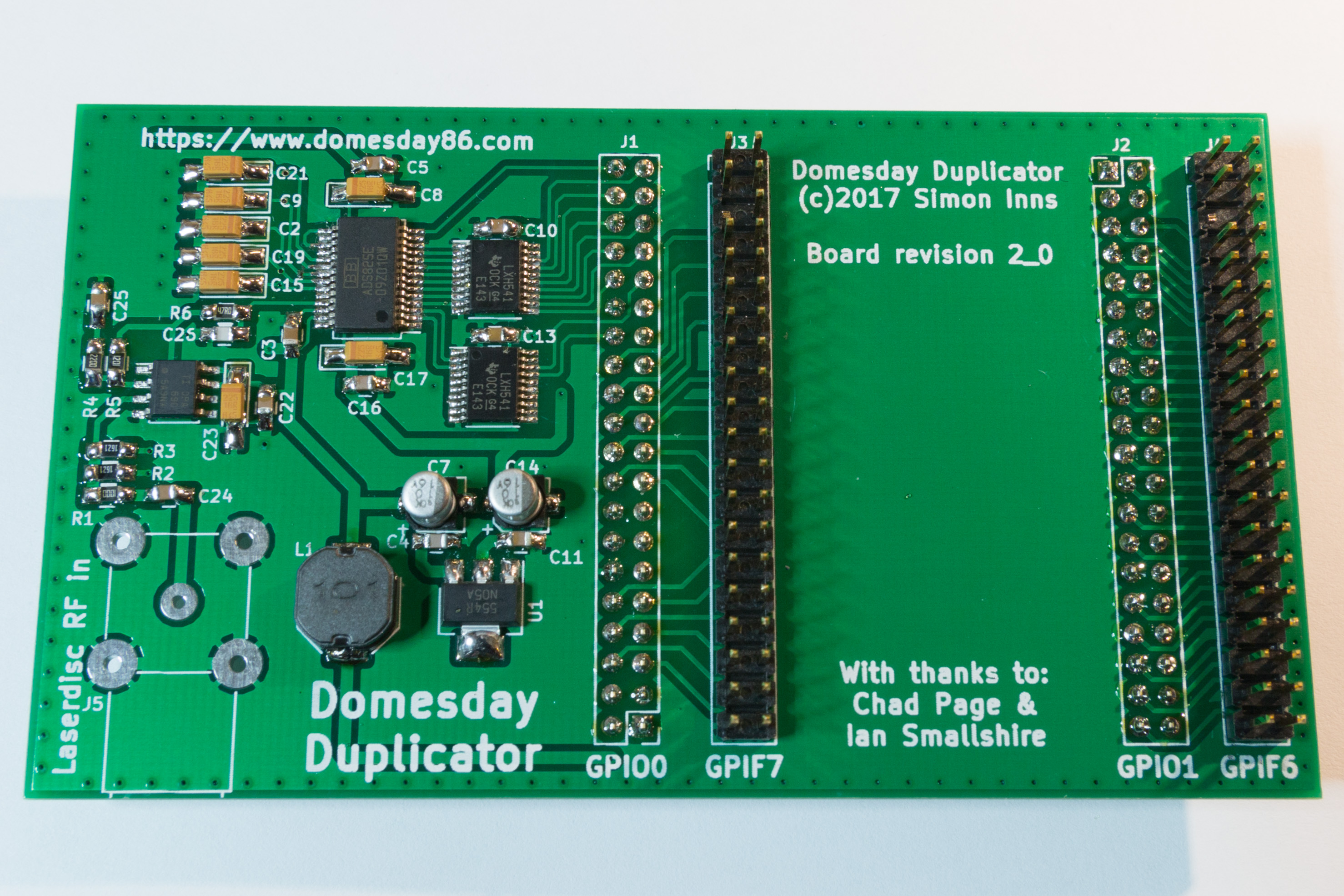
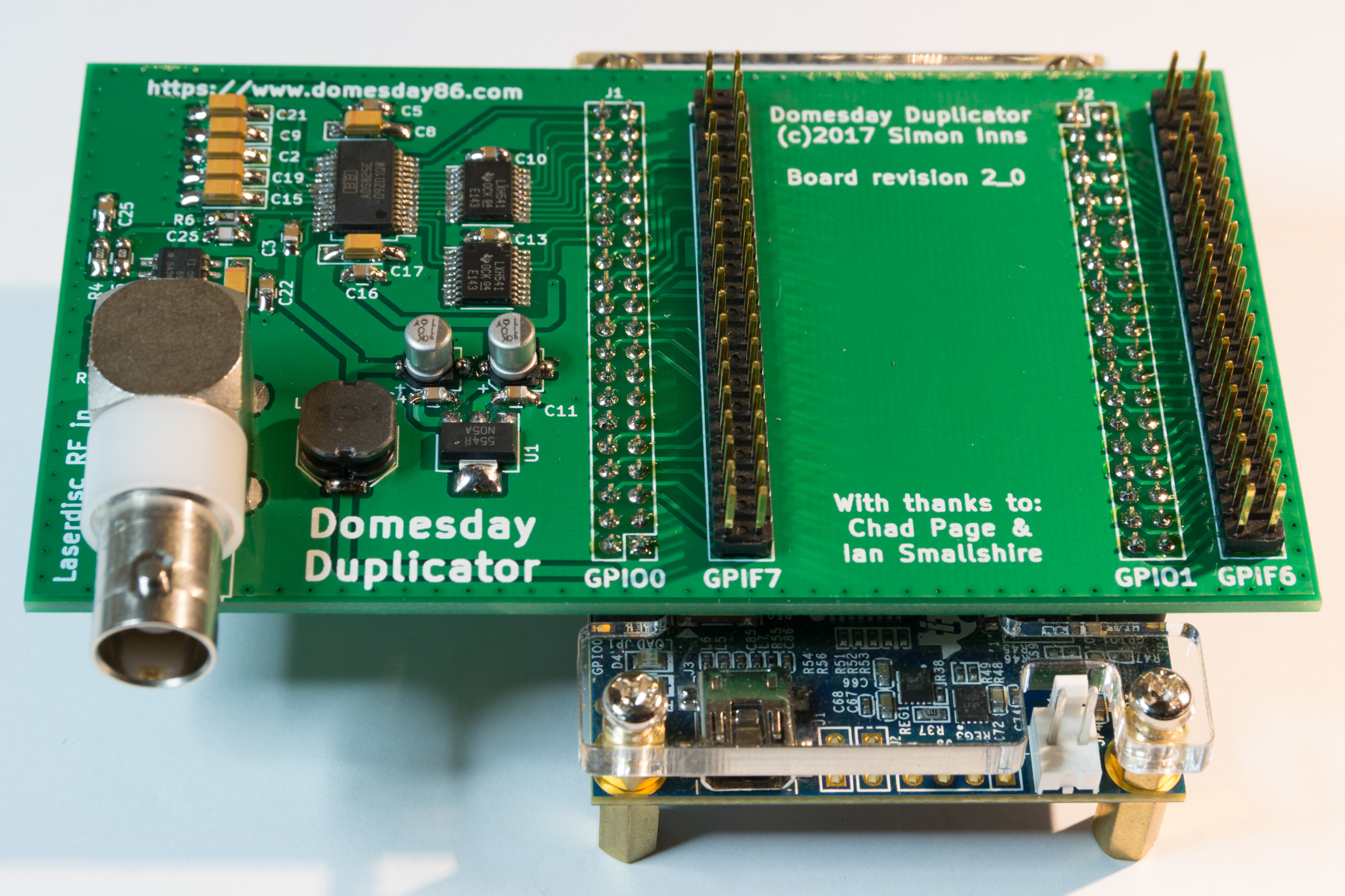
Domesday Duplicator PCB 2_0
This board revision has been superseded by the revision 3_0 PCB. Please see the Domesday Duplicator Hardware (3_0) page for more details.
This guide specifically covers revision 2_0 PCB boards. Please ensure that your board is marked with "Revision 2_0" before following this guide. The latest versions of all schematics and PCB designs can be found on Github.
Electronics design and schematics
RF Front-end
The RF front-end design can be seen in the following schematic diagram:
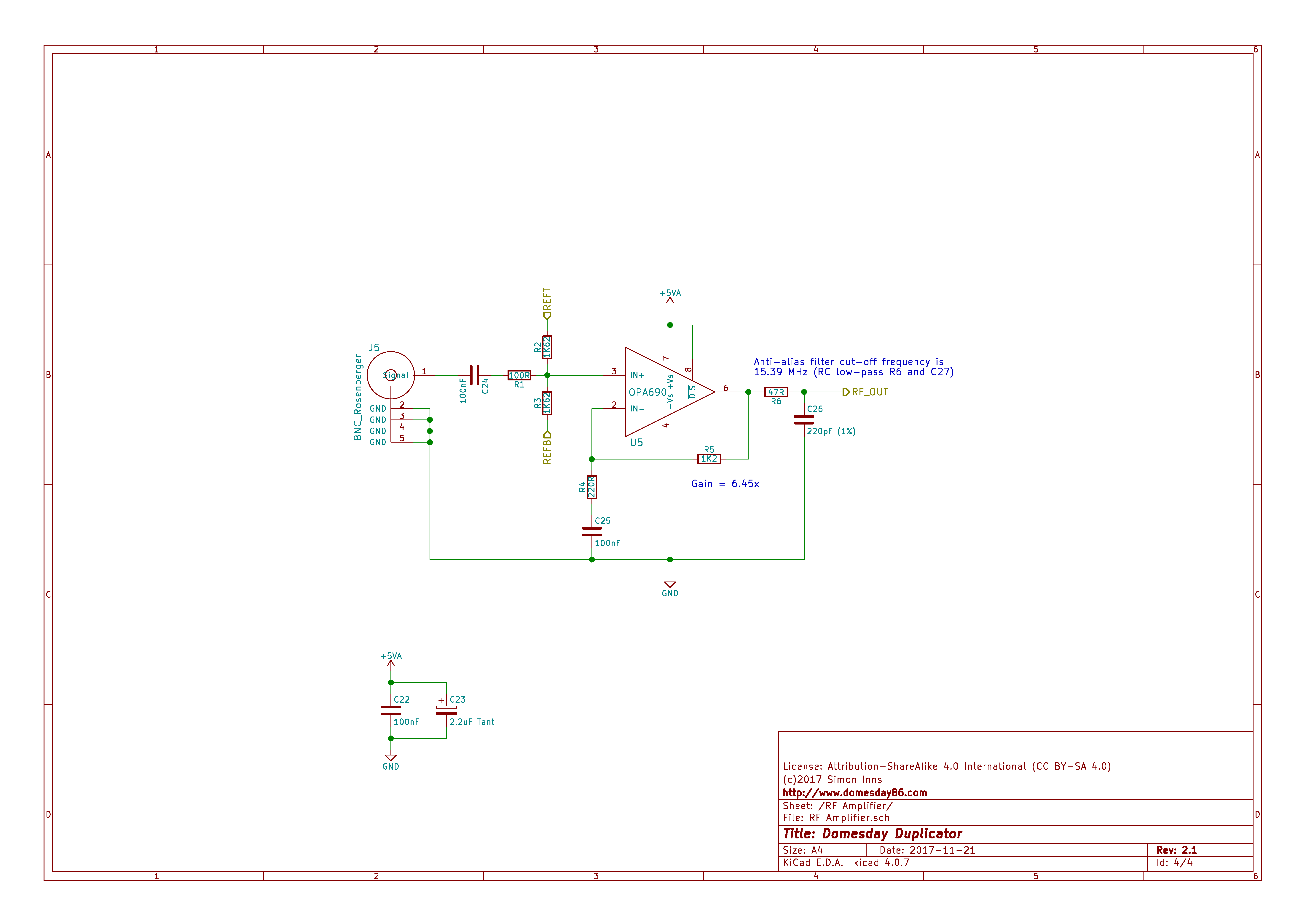
The RF front-end takes the raw RF output from the laserdisc player, decouples the DC offset and then applies a DC offset of 2.5V required for the ADC (note that the offset is provided by the ADC's reference signal generator (REFT and REFB)). A high-bandwidth OPA690 single-rail opamp is then used to add gain to the RF signal to ensure the amplitude of the RF is suitable for the 2V peak-to-peak range of the ADC. The OPA690 was chosen due to the high bandwidth and single-rail supply (allowing the Domesday Duplicator to be powered using only the 5V VBUS supply from the USB host).
For the Sony LDP-1500P laserdisc player R5 is set at 1K2 and R4 at 220R. This provides a gain of 6.45 suitable for the maximum peak RF signal of 300mV.
For the Pioneer LD-V43000D laserdisc player R5 is set at 1K and R4 at 270R. This provides a gain of 4.70 suitable for the maximum peak RF signal of 400mV.
Please note that the gain of the RF stage will be different for the various laserdisc models. There is no standard for the amplitude of the RF output from a player and, due to calibration, the RF gain may vary from player to player even of the same model. If in doubt, choose the values for 400mV signals as this provides a safer range for most players. Peak RF output to the ADC stage should not exceed 1800mV in normal operation for a good ADC result.
Measurement of the RF stage shows a consistent gain across a frequency range of 60KHz to 20MHz; signals above and below this range are attenuated by the circuitry. Given the expected frequency span of the laserdisc RF signal, the frequency response is more than adequate for the application.
The output from the RF front-end is passed through a simple RC low-pass filter with a cut-off frequency of approximately 15.4 MHz. This LPF acts as an anti-alias filter for the ADC stage (added to board revision 1_5 and above).
Modifying the RF front-end gain
For other laserdisc players it may be necessary to modify the gain of the RF front-end. The gain is set by two resistors R5 and R4. The rules for resistor selection are provided by the OPA690 datasheet:
R5 and R4 should be greater than 200 Ohms and less than 1500 Ohms.
The parallel combination of R5 and R4 should be less than 300 Ohms ( (R4 * R5) / (R4 + R5) = parallel combination resistance). So, (220 * 1200) / (220 + 1200) = 185.92 Ohms in the configuration shown by the schematic.
The overall gain is given by 1+(R5 / R4), so 1+(1200 / 220) = 6.45 in the configuration shown by the schematic.
10-bit ADC
The 10-bit ADC stage schematic can be seen in the following diagram:
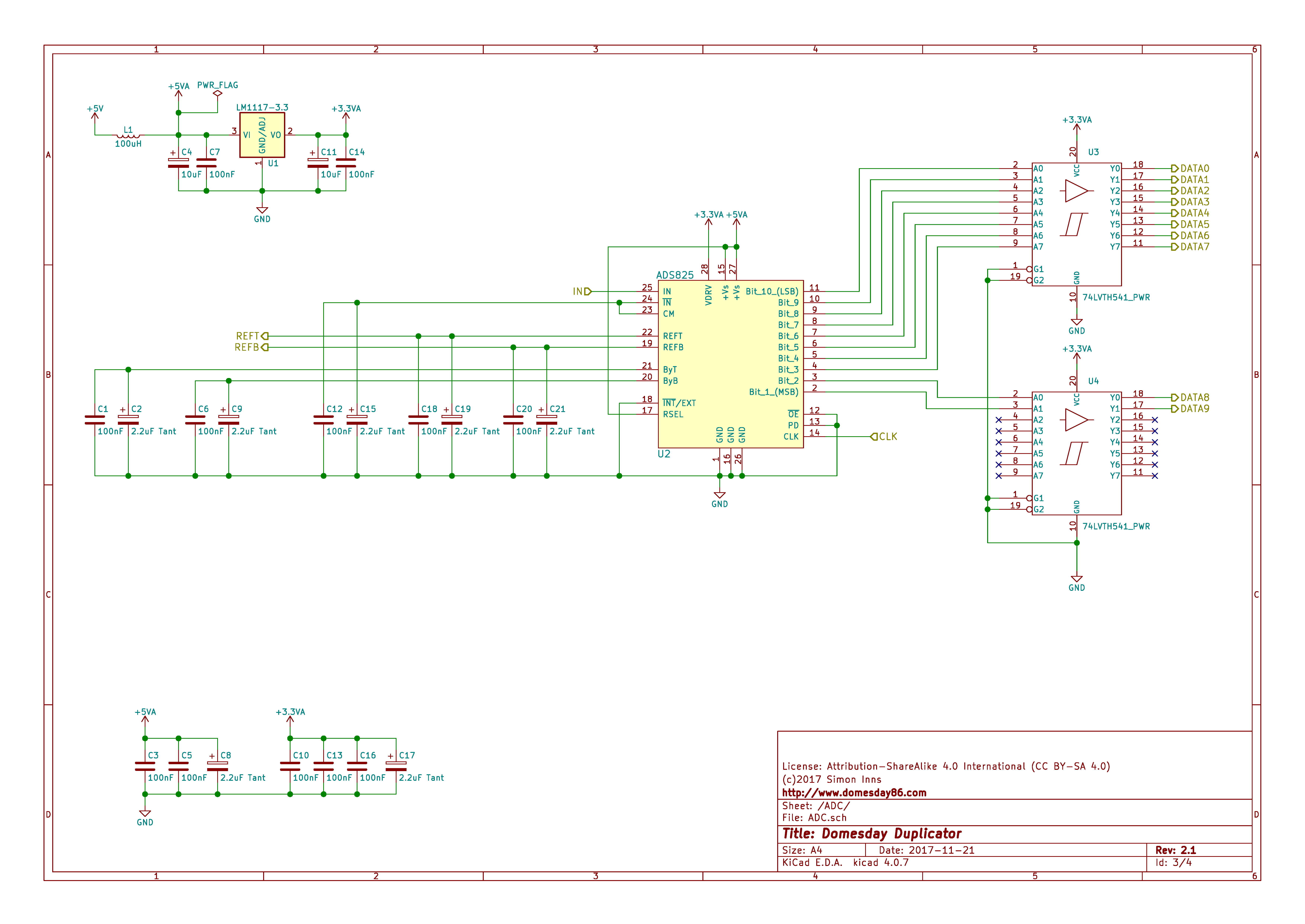
The ADC is a Texas Instruments ADS825 capable of 40 million samples per second (MSPS) at 10-bit resolution and provides a 10-bit parallel output. The ADC data generated by the ADS825 is an unsigned binary offset with 0 representing the lowest possible amplitude, 1023 as the maximum possible amplitude and 512 representing the centre point (DC offset of 0V) of the signal.
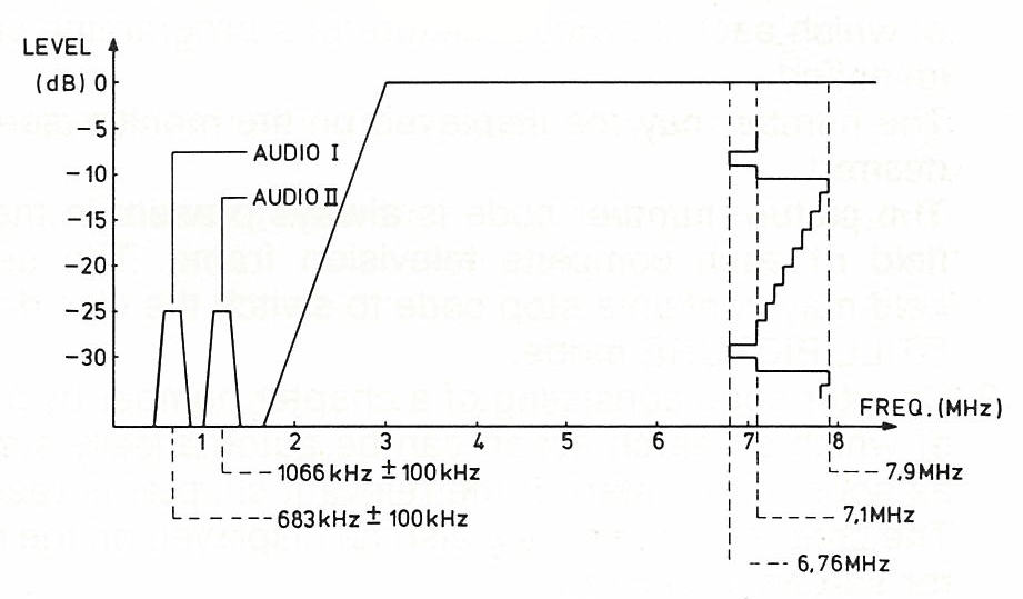
The expected signal from the laserdisc player is shown in the following diagram taken from the Philips VP415 service manual (note that this is for a PAL specific player):
Based on the highest expected Nyquist frequency of 8MHz the ADC must perform at least 16 MSPS in order to correctly sample the RF signal. Due to this the Domesday Duplicator uses a sampling rate of 32 MSPS (double the required sampling rate) to ensure accurate sampling of the signal. By doubling the maximum required sampling rate the loss of accuracy in the ADC due to 'windowing' is reduced.
Two line buffering ICs (74LVTH541) are used to buffer the output from the ADC towards the FPGA stage. These line buffers reduce the capacitive loading of the databus and effectively isolate the ADC from digital noise that can cause high-frequency interference in the analogue stages of the ADC. The design also provides power conditioning to ensure a smooth feed of both 5Vs and 3.3V to the ADC and RF front-end.
FPGA
Due to the unpredictable performance of a USB 3 interface an FPGA is used to act as a FIFO buffer between the ADC and the USB hardware. Although a modern PC can handle many times the bandwidth required by the application the bandwidth is not guaranteed (since a general purpose PC is not a real-time system, other system activities can cause the available bandwidth to vary).
The FPGA is provided by a DE0-Nano. The DE0-Nano is a low-cost FPGA development board from Terasic containing an Intel (Altera) Cyclone IV FPGA. The interconnection between the Domesday Duplicator and the FPGA development board is shown in the following schematic diagram:
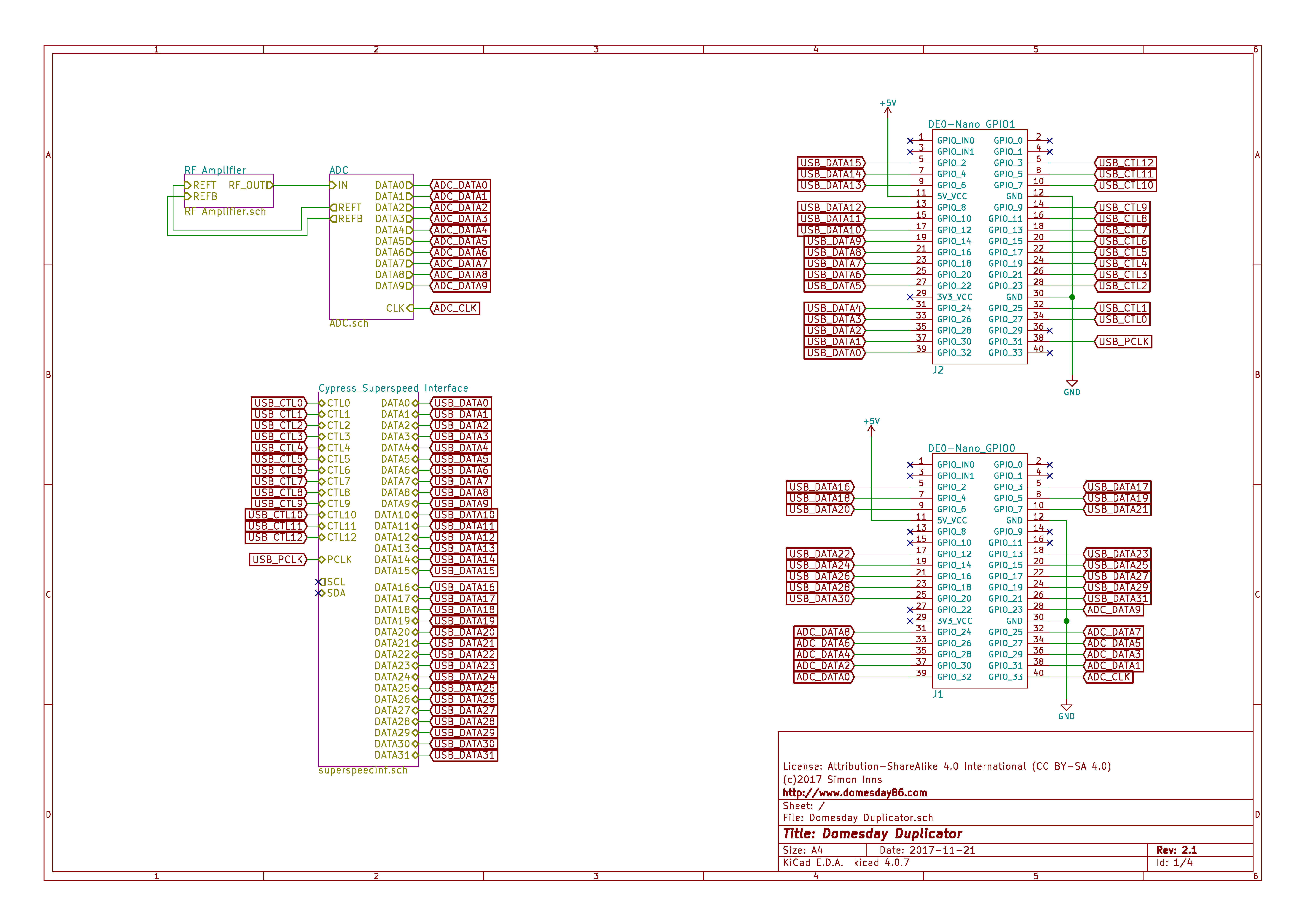
The FPGA uses a PLL function to provide a 32MHz clock to the ADC. Data from the ADC is collected by the FPGA into a 10-bit wide FIFO buffer. The FIFO buffer supports separate input and output clocking. The interface between the FPGA and the USB 3.0 interface is clocked at 64MHz. This dual-clock implementation allows the USB 3.0 to 'catch up' with the ADC data collection in the event of temporary loss of bandwidth.
In addition the FPGA changes the 10-bit unsigned FIFO output to scaled 16-bit signed data before passing the data to the USB 3.0 interface via a 16-bit databus. In addition to the databus the FPGA provides several additional control signals used to provide flow-control of the data between the FPGA and the USB 3.0 interface.
The data bandwidth from the FPGA to the USB 3.0 interface is a nominal 512Mbits/sec (16 bit words at 32 million words per second) or 61Mbytes/sec. Due to higher clock speed of the USB interface (64MHz) this can peak at 1024Mbits/sec as required.
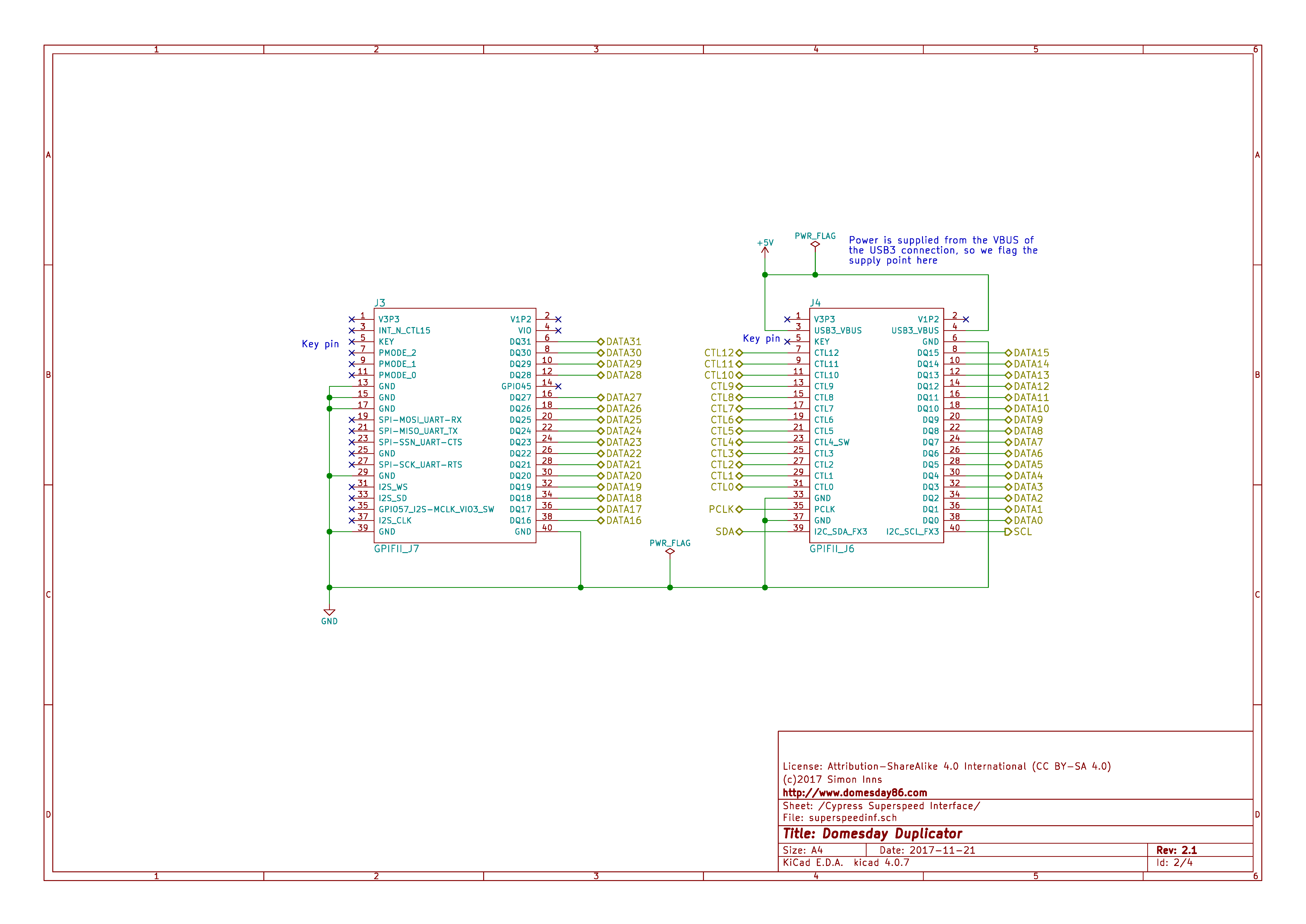
The design provides a full 32-bit data bus between the FPGA and the FX3 and 13 control lines. Currently only 16-bits of the data bus is used by the software (additional data bus and control signals are provided by the board to support future expansion).
USB 3.0 interface
The USB 3.0 interface between the FPGA and the host PC is provided by a Cypress SuperSpeed Explorer development board. This board provides a Cypress FX3 SuperSpeed USB 3.0 peripheral controller. USB 3 is required due to the data bandwidth requirement of the Domesday Duplicator (USB 2.0 only provides a realistic bandwidth of around 280Mbits/sec which is too low for the application). The FX3 provides a state-machine model (called GPIF II) that handles the transfer of data from the databus to the USB 3.0 interface and can run at a maximum of 100MHz (100 million words of 32-bit data per second). For the Domesday Duplicator, the FX3 is configured to use a 16-bit databus and the synchronous data clock is provided by the FPGA (at 64MHz).
The following schematic shows the interconnection to the FX3 board:
Bill of materials (BoM)
The Domesday Duplicator revision 2_0 PCB uses the following components:
| Ref | Qnty | Value | Footprint | Vendor | Article number |
| C2, C9, C15, C19, C21, C8, C17, C23 | 8 | 2.2uF Tant | EIA-3216-18 | RS Components | 648-0660 |
| C4, C11 | 2 | 10uF | Elec 4mm x 5.7mm | Distrelec | 167-310-21 |
| C12, C18, C1, C6, C7, C14, C3, C5, C10, C13, C16, C20, C24, C25, C22 | 15 | 100nF | 0805 | Distrelec | 300-65-839 |
| C26 | 1 | 220pF (1%) | 0805 | Distrelec | 300-66-258 |
| J1 | 1 | DE0-Nano_GPIO0 | Pin Header Straight 2x20 Pitch 2.54mm (female) | RS Components | 674-2369 |
| J2 | 1 | DE0-Nano_GPIO1 | Pin Header Straight 2x20 Pitch 2.54mm (female) | RS Components | 674-2369 |
| J3 | 1 | GPIFII_J7 | Pin Header Straight 2x20 Pitch 2.54mm | Distrelec | 143-83-934 |
| J4 | 1 | GPIFII_J6 | Pin Header Straight 2x20 Pitch 2.54mm | Distrelec | 143-83-934 |
| J5 | 1 | BNC_Rosenberger | BNC Socket - Rosenberger 51K204-400A5 | Distrelec | 146-44-967 |
| L1 | 1 | 100uH | Bourns SRN8040 Series SMD | RS Components | 743-5197 |
| R1 | 1 | 100R | 0805 | Distrelec | 300-56-716 |
| R2, R3 | 2 | 1K62 | 0805 | RS Components | 679-1027 |
| R4 | 1 | 220R | 0805 | Distrelec | 300-56-759 |
| R5 | 1 | 1K2 | 0805 | Distrelec | 300-56-729 |
| R6 | 1 | 47R | 0805 | Distrelec | 300-56-808 |
| U1 | 1 | LM1117-3.3 | SOT-223 | Distrelec | 300-19-198 |
| U2 | 1 | ADS825E | SSOP-28 5.3x10.2mm Pitch 0.65mm | RS Components | 662-0082 |
| U3, U4 | 2 | 74LVTH541_PWR | TSSOP-20 4.4x6.5mm Pitch 0.65mm | RS Components | 662-9187 |
| U5 | 1 | OPA690ID | SOIC-8 3.9x4.9mm Pitch 1.27mm | RS Components | 620-0082 |
PCB Assembly
Step 1: Mount the active components on the top-side of the board. Note the orientation of the integrated circuits; pin 1 is highlighted with a red dot.
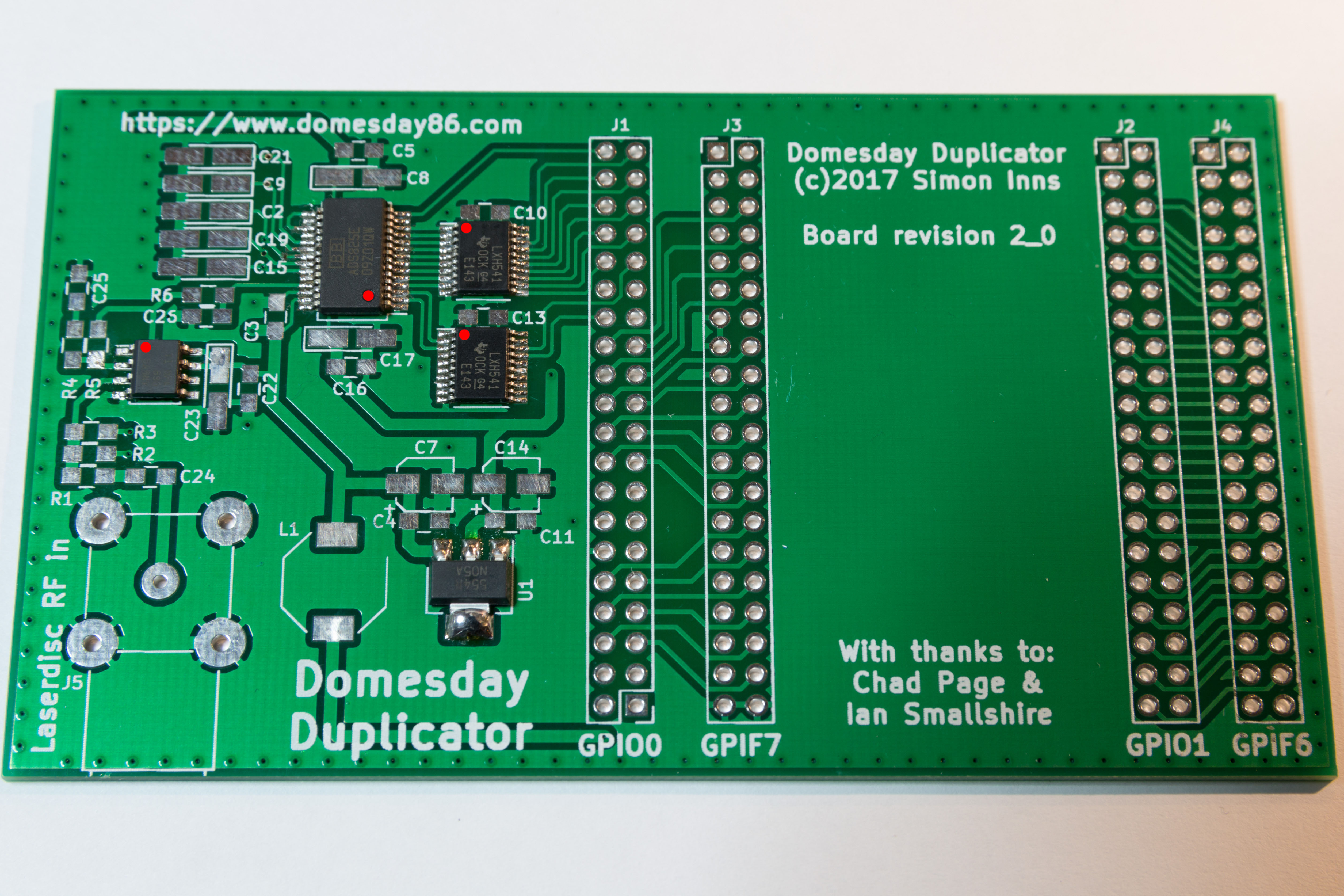
Step 2: Mount the 10x 100nF 0805 capacitors on the top-side of the board along with C26 (220pF)
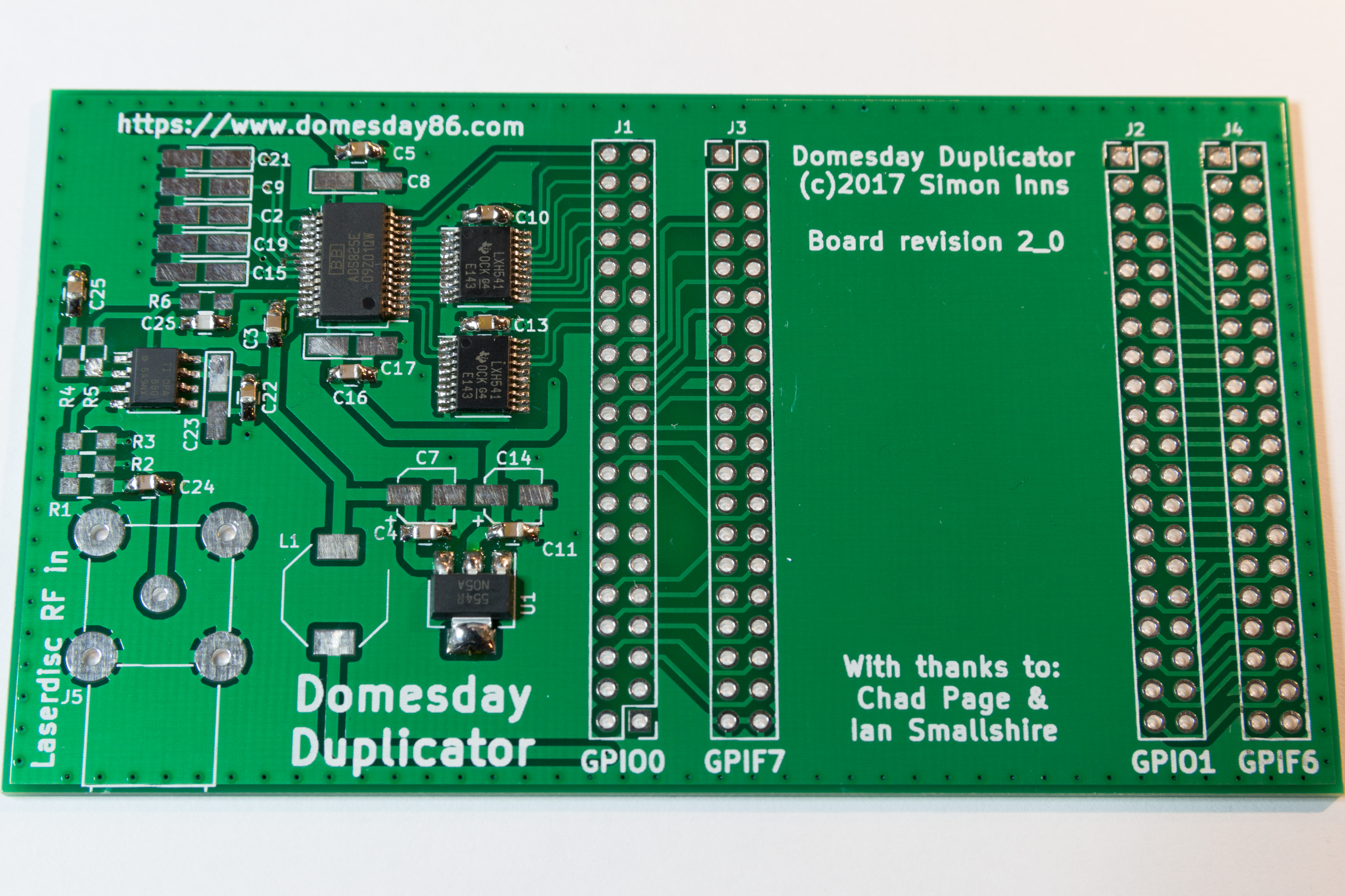
Step 3: Mount the 8x 2.2uf Tantalum capacitors on the top-side of the board. Note that these capacitors are polarized (the positive side is shown by the orange stripe). These must be orientated correctly.
Step 4: Mount the 6x 0805 resistors on the top-side of the board. Ensure the resistor values are correct according to the BoM (as they are all different values). The resistors should be R1 - 100R, R2 and R3 - 1K62, R4 - 220R, R5 - 1K2, R6 - 47R. Note that R4 and R5 control the RF gain and may be different for your laserdisc player. See the section "Modifying the front-end RF gain" above for details.
Step 5: 2x Electrolytic capacitors and inductor coil are fitted as shown below. Note that the capacitors are polarized and must be fitted the correct way round.
Step 6: Next mount the header pins (male top-side and female underside). Pin 3 of the male headers must be removed to allow insertion into the Cypress FX3 board which is keyed. On the underside of the board also mount the remaining 5x 100uF capacitors. Finally mount the BNC connector on the top-side of the board.
Step 7: Insert Domesday Duplicator into DE0-Nano FPGA development board being careful to correctly align the header pins. The board is orientated with the USB programming connector on the same side as the duplicator's BNC connector.
Step 8: Insert Cypress FX3 Superspeed development board onto Domesday Duplicator being careful to align the pins correctly. Note that pin 3 on either header is keyed and the FX3 board will only insert with the USB 3 connector to the rear of the duplicator.
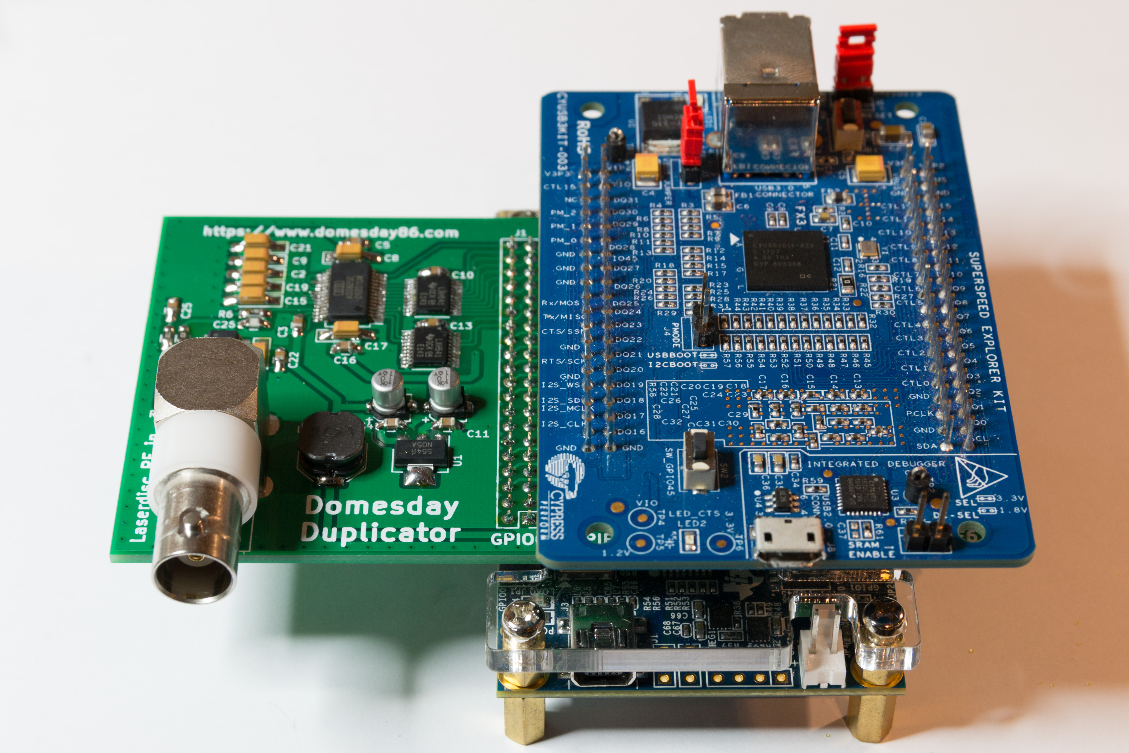
Once this final step is complete you will need to program both the FPGA and FX3. Please see the software guide for details.
Performance testing
RF Front-end
RF amplification
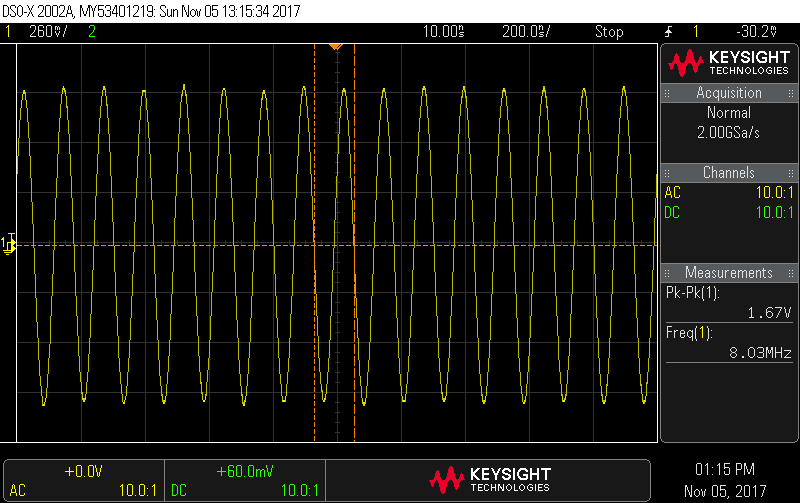
The following oscilloscope trace shows a 150mV peak-to-peak amplitude sine wave at 50 Ohms impedance at the BNC connector of the Domesday Duplicator (board revision 1_4):
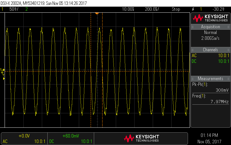
The following oscilloscope trace shows the same signal on the input (pin 3) to the OPA690 opamp:

The following oscilloscope trace shows the same signal on the input (pin 25) to the ADS825 ADC:
DC offset
The DC offset of the RF signal is provided by the ADS825's internal reference generator which is routed through two 1.62Kohm precision resistors to create the common-mode voltage which should be in the exact centre of the ADC's signal range. Testing against the revision 2_0 version of the board gave the following results:
- REFT = 3489mV
- REFB = 1509mV
- IN = 2491mV
With REFT-REFB = 1980mV the value at IN (with no input) should be (REFT-REFB) / 2 = 990mV above REFB, i.e. 2499mV. The value of IN under test was 2491mV which is within the expected range given the 1% tolerance of the precision resistors.
The ADC uses the not IN pin to act as the common-mode reference for the ADC process (when the ADS825 is used in a single-ended configuration). The ADS825 recommended configuration is to connect the CM output pin to not IN (with decoupling) to present the correct common-mode voltage for conversion (and this is the implementation on the revision 2_0 board). However, testing of the 2_0 board shows the CM pin provides a voltage of 2370mV; this is 129mV under the true common-mode voltage presented by REFT and REFB and causes the 2_0 revision board to read a positive DC-offset when sampling the inbound signal. This extra offset reduces the sensitivity of the ADC by 129mV on the positive-side of the incoming signal reducing the effective ADC range to 1851mV peak-to-peak.
Currently this unwanted offset is corrected by the FPGA software and care should be given not to exceed the reduced 1851mV peak-to-peak range. In the next version of the board it is likely that the addition of two more 1.62Kohm resistors on REFT and REFB should be used to generate the common-mode offset from the same source as the signal biasing and the CM should be simply decoupled to ground.
ADC performance
The following FFT graphs show a spectrum analysis of the Domesday Duplicator at the key PAL frequencies for a laserdisc. The input signal was a sine wave generated at 150mV peak-to-peak with 50Ohms impedance (board revision 1_4):
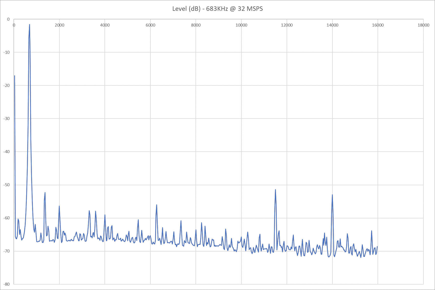
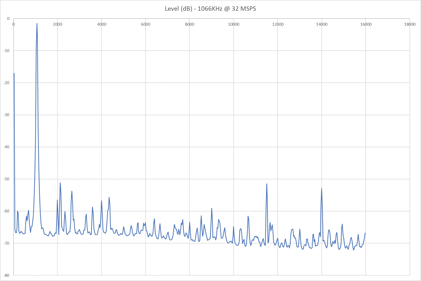
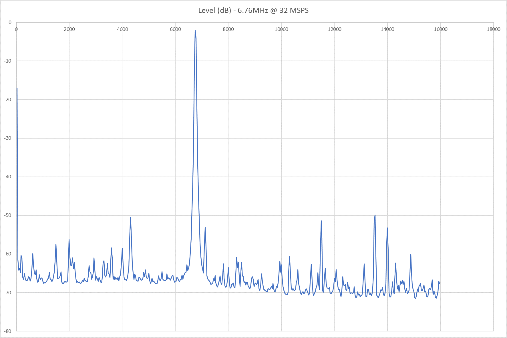
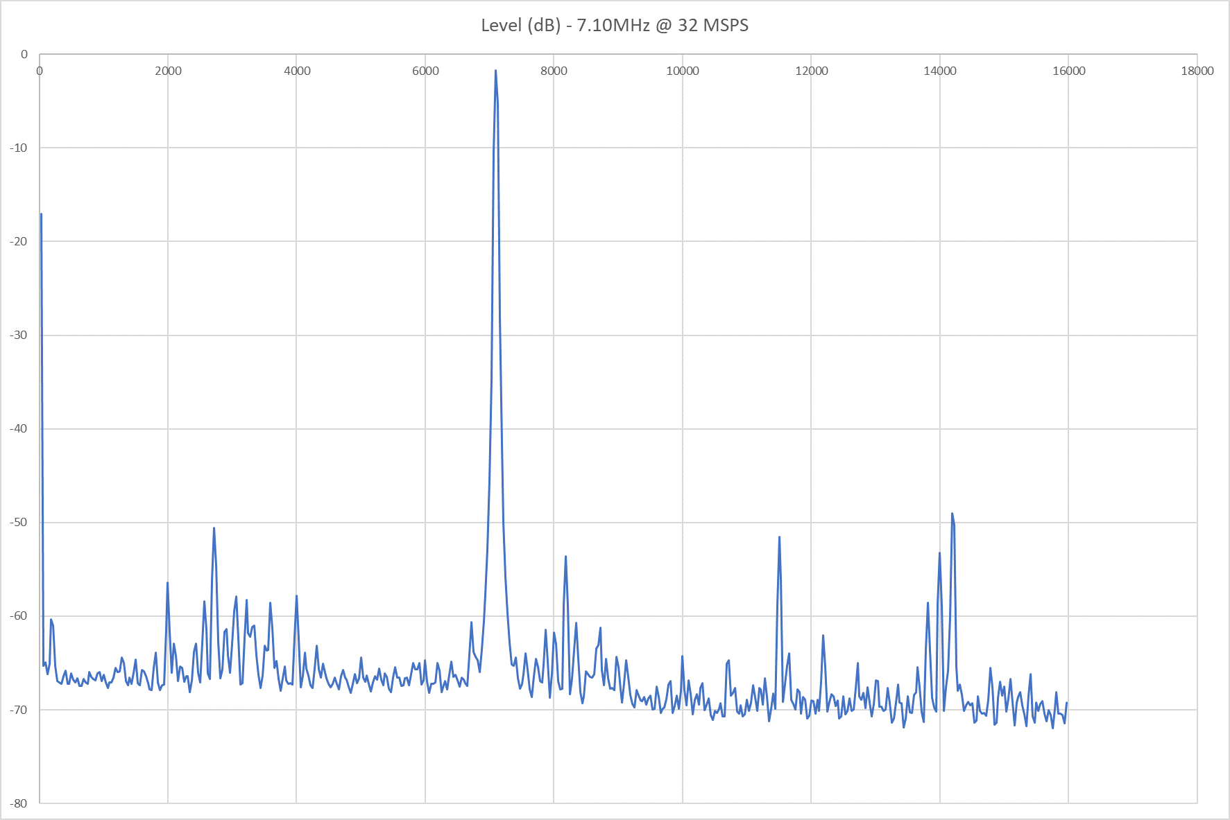
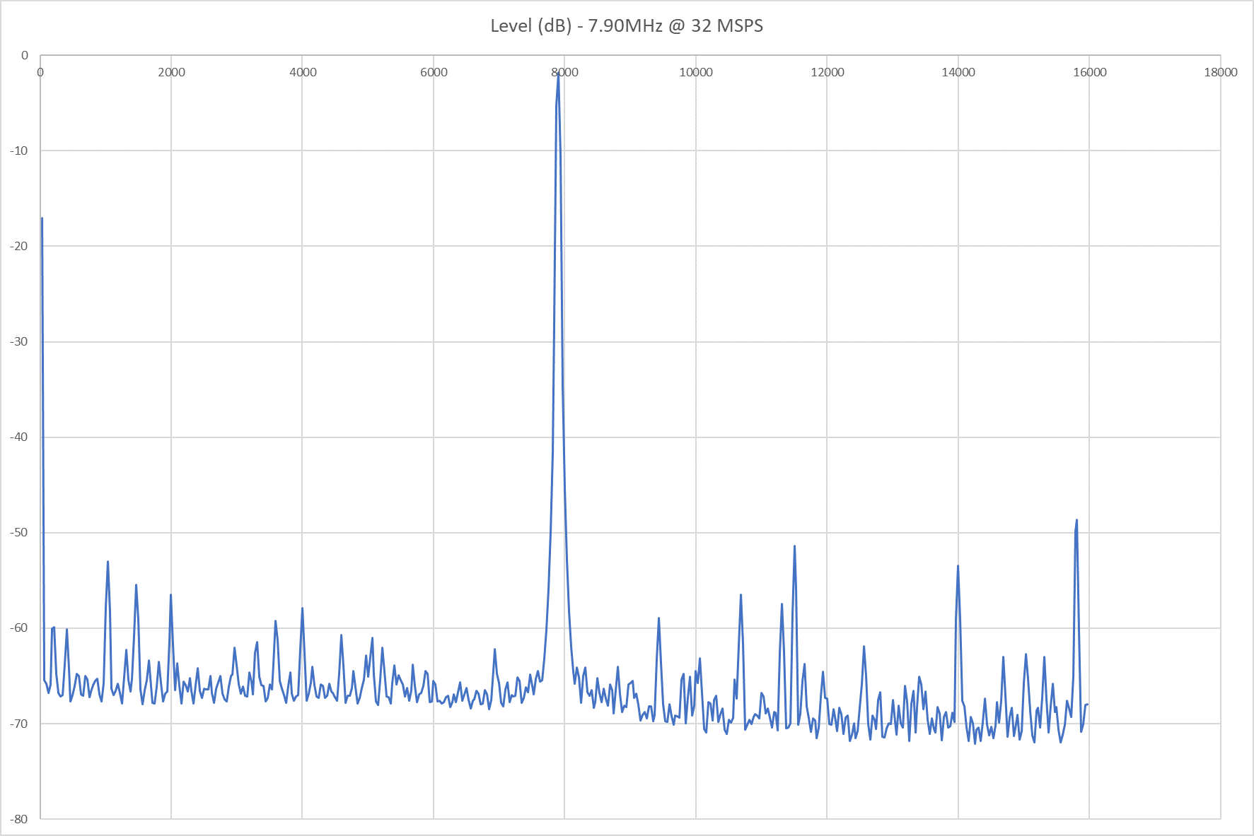
It can be seen from the FFT analysis that the peak amplitude of the signal is consistent over the required frequency range.
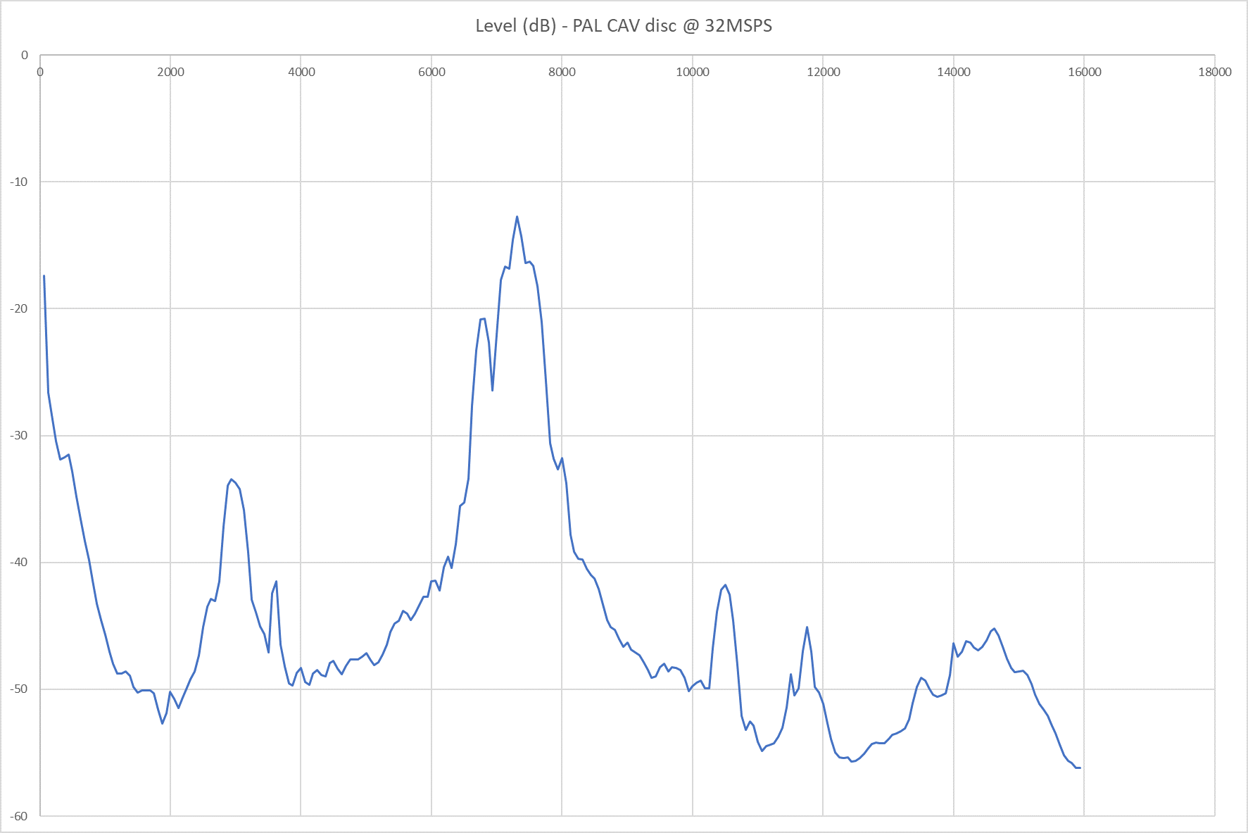
The following FFT shows a PAL CAV laserdisc signal from around the centre of the disc (note this disc contains only digital audio):